Texas Instruments LMK1D210xL Low Additive LVDS Buffers
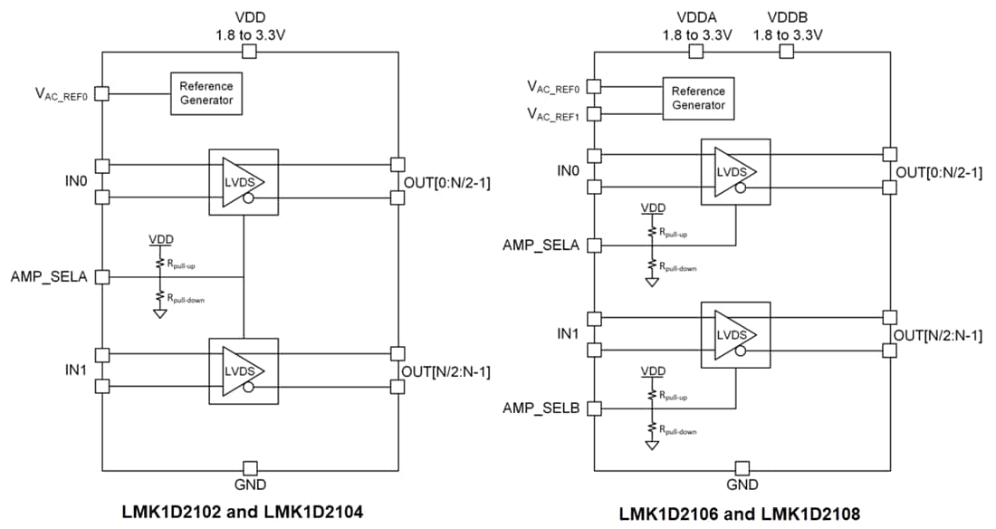
Texas Instruments LMK1D210xL Low-Additive LVDS Buffers are low noise dual clock buffers that distribute one input to a maximum of two (LMK1D2102L), four (LMK1D2104L), six (LMK1D2106L) or eight (LMK1D2108L) LVDS outputs. The inputs can be LVDS, LVPECL, HCSL, CML, or LVCMOS. The LMK1D210xL is designed explicitly for driving 50Ω transmission lines. When driving inputs in single-ended mode, apply the appropriate bias voltage to the unused negative input pin.The Texas Instruments LMK1D210xL buffer offers two output common mode operations (0.7V and 1.2V) for different operating supplies. The device provides flexibility in design for DC-coupled mode applications. AMP_SELA/AMP_SELB control pin can select different output amplitude LVDS (350mV) or boosted LVDS (500mV). In addition to amplitude selection, outputs can be disabled using the same pin. The part also supports the Fail-Safe Input function for the clock and digital input pins. The device further incorporates an input hysteresis, preventing random output oscillation without an input signal.
Features
- High-performance LVDS clock buffer family of up to 2GHz
- Dual 1:2 differential buffer
- Dual 1:4 differential buffer
- Dual 1:6 differential buffer
- Dual 1:8 differential buffer
- 1.71V to 3.465V supply voltage
- Dual output common mode voltage operation
- Output common mode voltage: 0.7V at 1.8V supply voltage.
- Output common mode voltage: 1.2V at 2.5V/3.3V supply voltage
- Low additive jitter
- < 17fs RMS typical in 12kHz to 20MHz at 1250.25MHz
- < 22fs RMS typical in 12kHz to 20MHz at 625MHz
- < 60fs RMS maximum in 12kHz to 20MHz at 156.25MHz
- Very low phase noise floor: -164dBc/Hz (typical at 156.25MHz)
- Very low propagation delay of < 575ps maximum
- Output skew:
- 15ps maximum (LMK1D2102, LMK1D2104)
- 20ps maximum (LMK1D2106, LMK1D2106)
- A part-to-part skew of 150ps
- High-swing LVDS (boosted mode) of 500mV VOD typical when AMP_SELA, AMP_SELB = Floating
- Bank enable/disable using AMP_SELA and AMP_SELB
- Fail-safe input operation
- Universal inputs accept LVDS, LVPECL, LVCMOS, HCSL, and CML signal levels
- LVDS reference voltage, VAC_REF, available for capacitive-coupled inputs
- –40°C to 105°C extended industrial temperature range
Applications
- Telecommunications and networking
- Medical imaging
- Test and measurement
- Wireless infrastructure
- Pro audio, video, and signage
Additional Resources
Functional Block Diagrams

Publicado: 2024-11-27
| Actualizado: 2025-03-21


