


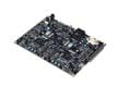
Lattice Semiconductor CrossLink-NX™ Evaluation Board
Lattice Semiconductor CrossLink-NX™ Evaluation Board is a demonstration and prototyping platform based on the CrossLink-NX Field Programmable Gate Array (FPGA). The CrossLink-NX evaluation board features the CrossLink-NX 40K LC FPGA in a 400-ball caBGA package (LIFCL-40-9BG400C). The Evaluation Board also features connectors for an FPGA Mezzanine Card (FMC) and a Raspberry Pi SBC. Additional headers for Digilent Peripheral Module (Pmod™), MIPI CSI-2 camera, D-PHY, and general-purpose I/O expansion are provided. With a 118 wide range I/O, 37 high-speed differential pair I/O, one PCIe 5G SERDES channel, and 40K Logic Cells available for user-defined applications, the Lattice Semiconductor CrossLink-NX evaluation board allows designers to thoroughly investigate and experiment with the features of the CrossLink-NX FPGA family.
CrossLink-NX
Built on the 28nm FD-SOI Lattice Nexus platform, the CrossLink-NX family of FPGAs lead their class in power, small form factor, reliability, and performance. These devices are optimized for a wide range of applications, including embedded vision, sensor and display bridging, sensor aggregation, sensor duplication, and AI inferencing at the Edge.
Features
- CrossLink-NX FPGA (LIFCL-40-9BG400C)
- General Purpose Input/Output (GPIO) breakout with Raspberry Pi, PMOD, and an FMC connector
- MIPI CSI-2 Camera connector and D-PHY connector
- 118 wide range I/O and 37 high-speed differential pair I/O with onboard termination
- USB-B connection for device programming and Inter-Integrated Circuit (I2C) utility
- Gen2 PCIe interface
- On-board Boot Flash – 128Mbit Serial Peripheral Interface (SPI) Flash, with a Quad read feature
- Eight input DIP switches, four pushbuttons, three status LEDs, and 14 LEDs for demo purposes
- Lattice Radiant® Software programming support
- Multiple reference clock sources
Related Products

Lattice Semiconductor CrossLink-NX™ VIP Sensor Input Board
Enables designers to experiment with the embedded vision features of the CrossLink-NX FPGA.

Lattice Semiconductor CrossLink-NX™ FPGAs
Built on the 28nm FD-SOI Lattice Nexus platform.
Lattice Semiconductor Sentry Demo Board
A 384-bit cryptography demonstration and test platform on a single board.
Videos
Board Layout

Configuration & I2C Architecture

Publicado: 2019-12-13
| Actualizado: 2023-04-17